Alumina Ceramic Substrates: The Foundational Enablers of High-Performance Electronic Packaging and Microsystem Integration in Modern Technology alumina silica refractory
1. Material Basics and Architectural Attributes of Alumina Ceramics
1.1 Crystallographic and Compositional Basis of α-Alumina
(Alumina Ceramic Substrates)
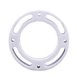
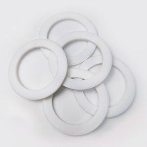
Alumina ceramic substratums, mainly made up of aluminum oxide (Al two O ₃), function as the foundation of modern-day electronic product packaging because of their phenomenal balance of electric insulation, thermal security, mechanical stamina, and manufacturability.
One of the most thermodynamically steady stage of alumina at high temperatures is corundum, or α-Al ₂ O FIVE, which takes shape in a hexagonal close-packed oxygen latticework with aluminum ions inhabiting two-thirds of the octahedral interstitial websites.
This thick atomic arrangement imparts high hardness (Mohs 9), exceptional wear resistance, and solid chemical inertness, making α-alumina suitable for rough operating atmospheres.
Business substratums generally have 90– 99.8% Al Two O FOUR, with small enhancements of silica (SiO ₂), magnesia (MgO), or uncommon planet oxides made use of as sintering help to advertise densification and control grain growth throughout high-temperature handling.
Higher purity qualities (e.g., 99.5% and over) exhibit exceptional electrical resistivity and thermal conductivity, while lower pureness versions (90– 96%) provide economical remedies for much less demanding applications.
1.2 Microstructure and Issue Design for Electronic Dependability
The efficiency of alumina substratums in electronic systems is critically dependent on microstructural uniformity and defect minimization.
A penalty, equiaxed grain structure– commonly ranging from 1 to 10 micrometers– makes sure mechanical integrity and decreases the chance of fracture breeding under thermal or mechanical anxiety.
Porosity, particularly interconnected or surface-connected pores, need to be reduced as it deteriorates both mechanical toughness and dielectric performance.
Advanced processing strategies such as tape casting, isostatic pressing, and regulated sintering in air or controlled ambiences allow the manufacturing of substratums with near-theoretical density (> 99.5%) and surface roughness below 0.5 µm, vital for thin-film metallization and cable bonding.
In addition, pollutant segregation at grain borders can result in leakage currents or electrochemical migration under predisposition, demanding rigorous control over raw material pureness and sintering problems to ensure lasting reliability in damp or high-voltage settings.
2. Production Processes and Substrate Manufacture Technologies
( Alumina Ceramic Substrates)
2.1 Tape Casting and Eco-friendly Body Handling
The production of alumina ceramic substrates starts with the preparation of an extremely distributed slurry including submicron Al ₂ O five powder, organic binders, plasticizers, dispersants, and solvents.
This slurry is refined via tape spreading– a continuous approach where the suspension is topped a moving provider film utilizing an accuracy doctor blade to accomplish consistent density, normally in between 0.1 mm and 1.0 mm.
After solvent dissipation, the resulting “eco-friendly tape” is versatile and can be punched, drilled, or laser-cut to form using holes for vertical affiliations.
Numerous layers may be laminated flooring to develop multilayer substratums for complicated circuit integration, although most of commercial applications utilize single-layer arrangements due to set you back and thermal expansion factors to consider.
The green tapes are then meticulously debound to remove organic ingredients with managed thermal decomposition before final sintering.
2.2 Sintering and Metallization for Circuit Combination
Sintering is conducted in air at temperature levels between 1550 ° C and 1650 ° C, where solid-state diffusion drives pore removal and grain coarsening to attain complete densification.
The straight shrinking during sintering– typically 15– 20%– have to be exactly predicted and made up for in the style of eco-friendly tapes to ensure dimensional accuracy of the final substrate.
Adhering to sintering, metallization is put on develop conductive traces, pads, and vias.
Two main methods dominate: thick-film printing and thin-film deposition.
In thick-film modern technology, pastes having metal powders (e.g., tungsten, molybdenum, or silver-palladium alloys) are screen-printed onto the substrate and co-fired in a minimizing atmosphere to form durable, high-adhesion conductors.
For high-density or high-frequency applications, thin-film processes such as sputtering or dissipation are used to down payment attachment layers (e.g., titanium or chromium) followed by copper or gold, allowing sub-micron patterning via photolithography.
Vias are loaded with conductive pastes and terminated to develop electrical interconnections between layers in multilayer styles.
3. Useful Properties and Performance Metrics in Electronic Solution
3.1 Thermal and Electrical Actions Under Operational Tension
Alumina substratums are prized for their desirable combination of moderate thermal conductivity (20– 35 W/m · K for 96– 99.8% Al ₂ O THREE), which allows efficient warmth dissipation from power tools, and high volume resistivity (> 10 ¹⁴ Ω · centimeters), making sure very little leak current.
Their dielectric constant (εᵣ ≈ 9– 10 at 1 MHz) is steady over a broad temperature and frequency range, making them appropriate for high-frequency circuits up to numerous gigahertz, although lower-κ materials like light weight aluminum nitride are preferred for mm-wave applications.
The coefficient of thermal expansion (CTE) of alumina (~ 6.8– 7.2 ppm/K) is fairly well-matched to that of silicon (~ 3 ppm/K) and specific packaging alloys, minimizing thermo-mechanical anxiety throughout device operation and thermal cycling.
Nevertheless, the CTE inequality with silicon continues to be a concern in flip-chip and direct die-attach configurations, typically needing compliant interposers or underfill products to reduce exhaustion failure.
3.2 Mechanical Toughness and Ecological Toughness
Mechanically, alumina substrates display high flexural strength (300– 400 MPa) and superb dimensional security under load, enabling their use in ruggedized electronic devices for aerospace, automobile, and commercial control systems.
They are resistant to resonance, shock, and creep at elevated temperature levels, keeping structural honesty up to 1500 ° C in inert atmospheres.
In humid settings, high-purity alumina reveals minimal wetness absorption and outstanding resistance to ion movement, making certain long-lasting dependability in exterior and high-humidity applications.
Surface area hardness also safeguards versus mechanical damage during handling and assembly, although treatment should be required to stay clear of side breaking as a result of intrinsic brittleness.
4. Industrial Applications and Technological Effect Throughout Sectors
4.1 Power Electronics, RF Modules, and Automotive Solutions
Alumina ceramic substrates are common in power digital components, consisting of shielded entrance bipolar transistors (IGBTs), MOSFETs, and rectifiers, where they offer electric seclusion while assisting in heat transfer to warmth sinks.
In superhigh frequency (RF) and microwave circuits, they function as service provider platforms for crossbreed incorporated circuits (HICs), surface acoustic wave (SAW) filters, and antenna feed networks because of their stable dielectric properties and low loss tangent.
In the vehicle market, alumina substratums are made use of in engine control systems (ECUs), sensing unit bundles, and electrical car (EV) power converters, where they withstand high temperatures, thermal biking, and direct exposure to destructive fluids.
Their reliability under extreme problems makes them essential for safety-critical systems such as anti-lock braking (ABDOMINAL) and advanced chauffeur support systems (ADAS).
4.2 Medical Instruments, Aerospace, and Arising Micro-Electro-Mechanical Equipments
Beyond consumer and commercial electronic devices, alumina substrates are used in implantable clinical devices such as pacemakers and neurostimulators, where hermetic securing and biocompatibility are vital.
In aerospace and defense, they are made use of in avionics, radar systems, and satellite interaction components as a result of their radiation resistance and security in vacuum cleaner environments.
Additionally, alumina is significantly utilized as an architectural and shielding platform in micro-electro-mechanical systems (MEMS), including pressure sensors, accelerometers, and microfluidic tools, where its chemical inertness and compatibility with thin-film handling are useful.
As electronic systems continue to demand higher power thickness, miniaturization, and integrity under severe conditions, alumina ceramic substrates remain a cornerstone material, bridging the gap in between efficiency, price, and manufacturability in advanced digital packaging.
5. Vendor
Alumina Technology Co., Ltd focus on the research and development, production and sales of aluminum oxide powder, aluminum oxide products, aluminum oxide crucible, etc., serving the electronics, ceramics, chemical and other industries. Since its establishment in 2005, the company has been committed to providing customers with the best products and services. If you are looking for high quality alumina silica refractory, please feel free to contact us. (nanotrun@yahoo.com)
Tags: Alumina Ceramic Substrates, Alumina Ceramics, alumina
All articles and pictures are from the Internet. If there are any copyright issues, please contact us in time to delete.
Inquiry us
