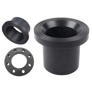
Silicon Carbide Ceramics: High-Performance Materials for Extreme Environment Applications alumina refractory
1. Crystal Structure and Polytypism of Silicon Carbide
1.1 Cubic and Hexagonal Polytypes: From 3C to 6H and Beyond
(Silicon Carbide Ceramics)
Silicon carbide (SiC) is a covalently bonded ceramic composed of silicon and carbon atoms prepared in a tetrahedral control, creating one of one of the most complex systems of polytypism in materials scientific research.
Unlike many porcelains with a single secure crystal framework, SiC exists in over 250 well-known polytypes– unique stacking series of close-packed Si-C bilayers along the c-axis– varying from cubic 3C-SiC (also known as β-SiC) to hexagonal 6H-SiC and rhombohedral 15R-SiC.
One of the most common polytypes used in engineering applications are 3C (cubic), 4H, and 6H (both hexagonal), each showing a little different electronic band structures and thermal conductivities.
3C-SiC, with its zinc blende structure, has the narrowest bandgap (~ 2.3 eV) and is commonly grown on silicon substratums for semiconductor gadgets, while 4H-SiC provides remarkable electron mobility and is preferred for high-power electronic devices.
The solid covalent bonding and directional nature of the Si– C bond give exceptional solidity, thermal security, and resistance to sneak and chemical attack, making SiC perfect for extreme environment applications.
1.2 Problems, Doping, and Electronic Feature
In spite of its architectural intricacy, SiC can be doped to achieve both n-type and p-type conductivity, enabling its use in semiconductor gadgets.
Nitrogen and phosphorus function as donor contaminations, introducing electrons into the transmission band, while light weight aluminum and boron act as acceptors, producing openings in the valence band.
Nonetheless, p-type doping efficiency is limited by high activation energies, especially in 4H-SiC, which positions challenges for bipolar device style.
Native problems such as screw dislocations, micropipes, and stacking faults can deteriorate tool performance by acting as recombination facilities or leakage paths, demanding premium single-crystal growth for digital applications.
The wide bandgap (2.3– 3.3 eV relying on polytype), high malfunction electric area (~ 3 MV/cm), and exceptional thermal conductivity (~ 3– 4 W/m · K for 4H-SiC) make SiC much superior to silicon in high-temperature, high-voltage, and high-frequency power electronics.
2. Handling and Microstructural Engineering
( Silicon Carbide Ceramics)
2.1 Sintering and Densification Strategies
Silicon carbide is inherently hard to densify due to its solid covalent bonding and reduced self-diffusion coefficients, needing sophisticated handling methods to achieve full density without additives or with marginal sintering help.
Pressureless sintering of submicron SiC powders is possible with the addition of boron and carbon, which advertise densification by eliminating oxide layers and boosting solid-state diffusion.
Warm pressing uses uniaxial pressure during heating, enabling full densification at reduced temperatures (~ 1800– 2000 ° C )and producing fine-grained, high-strength components appropriate for cutting devices and put on parts.
For large or complicated shapes, reaction bonding is utilized, where porous carbon preforms are infiltrated with molten silicon at ~ 1600 ° C, forming β-SiC sitting with very little shrinking.
Nevertheless, recurring cost-free silicon (~ 5– 10%) stays in the microstructure, restricting high-temperature performance and oxidation resistance above 1300 ° C.
2.2 Additive Production and Near-Net-Shape Construction
Current breakthroughs in additive production (AM), especially binder jetting and stereolithography making use of SiC powders or preceramic polymers, make it possible for the fabrication of intricate geometries formerly unattainable with standard methods.
In polymer-derived ceramic (PDC) routes, fluid SiC precursors are shaped by means of 3D printing and then pyrolyzed at high temperatures to produce amorphous or nanocrystalline SiC, typically calling for more densification.
These methods minimize machining costs and material waste, making SiC extra obtainable for aerospace, nuclear, and warmth exchanger applications where complex layouts enhance performance.
Post-processing actions such as chemical vapor seepage (CVI) or liquid silicon infiltration (LSI) are often used to boost thickness and mechanical honesty.
3. Mechanical, Thermal, and Environmental Performance
3.1 Stamina, Solidity, and Wear Resistance
Silicon carbide places amongst the hardest recognized materials, with a Mohs firmness of ~ 9.5 and Vickers hardness going beyond 25 GPa, making it highly resistant to abrasion, disintegration, and scratching.
Its flexural strength usually ranges from 300 to 600 MPa, relying on processing approach and grain dimension, and it maintains stamina at temperatures approximately 1400 ° C in inert ambiences.
Crack durability, while modest (~ 3– 4 MPa · m ONE/ ²), is sufficient for several structural applications, especially when combined with fiber support in ceramic matrix compounds (CMCs).
SiC-based CMCs are used in generator blades, combustor liners, and brake systems, where they supply weight financial savings, gas performance, and expanded service life over metallic counterparts.
Its excellent wear resistance makes SiC suitable for seals, bearings, pump elements, and ballistic shield, where sturdiness under harsh mechanical loading is important.
3.2 Thermal Conductivity and Oxidation Stability
One of SiC’s most beneficial properties is its high thermal conductivity– as much as 490 W/m · K for single-crystal 4H-SiC and ~ 30– 120 W/m · K for polycrystalline forms– exceeding that of lots of metals and enabling effective warmth dissipation.
This residential property is essential in power electronics, where SiC gadgets generate much less waste heat and can operate at greater power densities than silicon-based devices.
At raised temperatures in oxidizing settings, SiC forms a protective silica (SiO ₂) layer that slows down further oxidation, offering great ecological sturdiness up to ~ 1600 ° C.
Nevertheless, in water vapor-rich atmospheres, this layer can volatilize as Si(OH)FOUR, leading to accelerated deterioration– a vital difficulty in gas generator applications.
4. Advanced Applications in Energy, Electronic Devices, and Aerospace
4.1 Power Electronics and Semiconductor Tools
Silicon carbide has reinvented power electronics by allowing tools such as Schottky diodes, MOSFETs, and JFETs that operate at higher voltages, regularities, and temperatures than silicon matchings.
These devices lower energy losses in electrical automobiles, renewable energy inverters, and industrial motor drives, adding to global energy efficiency renovations.
The ability to operate at joint temperatures over 200 ° C allows for streamlined air conditioning systems and enhanced system dependability.
Additionally, SiC wafers are made use of as substrates for gallium nitride (GaN) epitaxy in high-electron-mobility transistors (HEMTs), incorporating the benefits of both wide-bandgap semiconductors.
4.2 Nuclear, Aerospace, and Optical Solutions
In atomic power plants, SiC is a vital component of accident-tolerant fuel cladding, where its low neutron absorption cross-section, radiation resistance, and high-temperature stamina boost safety and efficiency.
In aerospace, SiC fiber-reinforced composites are made use of in jet engines and hypersonic cars for their light-weight and thermal security.
Furthermore, ultra-smooth SiC mirrors are utilized precede telescopes because of their high stiffness-to-density proportion, thermal security, and polishability to sub-nanometer roughness.
In recap, silicon carbide ceramics stand for a foundation of contemporary innovative products, combining phenomenal mechanical, thermal, and electronic properties.
With accurate control of polytype, microstructure, and processing, SiC continues to make it possible for technical innovations in energy, transport, and severe environment engineering.
5. Supplier
TRUNNANO is a supplier of Spherical Tungsten Powder with over 12 years of experience in nano-building energy conservation and nanotechnology development. It accepts payment via Credit Card, T/T, West Union and Paypal. Trunnano will ship the goods to customers overseas through FedEx, DHL, by air, or by sea. If you want to know more about Spherical Tungsten Powder, please feel free to contact us and send an inquiry(sales5@nanotrun.com).
Tags: silicon carbide ceramic,silicon carbide ceramic products, industry ceramic
All articles and pictures are from the Internet. If there are any copyright issues, please contact us in time to delete.
Inquiry us
