Spherical Silica: Precision Engineered Particles for Advanced Material Applications silicon is a semiconductor
1. Architectural Features and Synthesis of Spherical Silica
1.1 Morphological Interpretation and Crystallinity
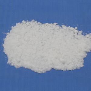
(Spherical Silica)
Round silica describes silicon dioxide (SiO TWO) bits engineered with a very uniform, near-perfect spherical shape, differentiating them from standard irregular or angular silica powders originated from all-natural sources.
These particles can be amorphous or crystalline, though the amorphous kind controls commercial applications because of its exceptional chemical security, reduced sintering temperature level, and absence of stage changes that can induce microcracking.
The spherical morphology is not naturally common; it must be synthetically attained through managed processes that control nucleation, growth, and surface area power reduction.
Unlike crushed quartz or fused silica, which display jagged edges and wide dimension circulations, round silica attributes smooth surface areas, high packaging density, and isotropic actions under mechanical stress, making it suitable for accuracy applications.
The particle size generally varies from tens of nanometers to several micrometers, with limited control over size distribution making it possible for foreseeable performance in composite systems.
1.2 Regulated Synthesis Pathways
The main approach for generating round silica is the Stöber process, a sol-gel method developed in the 1960s that includes the hydrolysis and condensation of silicon alkoxides– most typically tetraethyl orthosilicate (TEOS)– in an alcoholic service with ammonia as a catalyst.
By changing specifications such as reactant focus, water-to-alkoxide proportion, pH, temperature, and reaction time, researchers can exactly tune particle dimension, monodispersity, and surface area chemistry.
This method returns extremely uniform, non-agglomerated balls with outstanding batch-to-batch reproducibility, vital for state-of-the-art production.
Alternative methods include flame spheroidization, where uneven silica bits are melted and improved into balls via high-temperature plasma or fire treatment, and emulsion-based methods that allow encapsulation or core-shell structuring.
For massive industrial production, sodium silicate-based rainfall routes are also utilized, using cost-effective scalability while keeping appropriate sphericity and purity.
Surface area functionalization throughout or after synthesis– such as grafting with silanes– can present organic teams (e.g., amino, epoxy, or vinyl) to enhance compatibility with polymer matrices or allow bioconjugation.
( Spherical Silica)
2. Useful Qualities and Performance Advantages
2.1 Flowability, Packing Density, and Rheological Habits
Among the most substantial advantages of spherical silica is its exceptional flowability contrasted to angular counterparts, a building important in powder handling, injection molding, and additive manufacturing.
The absence of sharp edges lowers interparticle rubbing, enabling dense, homogeneous packing with very little void room, which enhances the mechanical stability and thermal conductivity of final compounds.
In digital product packaging, high packaging density directly equates to lower resin web content in encapsulants, enhancing thermal security and reducing coefficient of thermal growth (CTE).
Furthermore, round particles convey beneficial rheological buildings to suspensions and pastes, decreasing thickness and preventing shear enlarging, which guarantees smooth giving and consistent covering in semiconductor manufacture.
This controlled flow habits is indispensable in applications such as flip-chip underfill, where accurate material placement and void-free dental filling are called for.
2.2 Mechanical and Thermal Security
Round silica displays excellent mechanical toughness and elastic modulus, contributing to the support of polymer matrices without causing tension focus at sharp corners.
When included right into epoxy resins or silicones, it improves solidity, wear resistance, and dimensional stability under thermal cycling.
Its low thermal expansion coefficient (~ 0.5 × 10 ⁻⁶/ K) closely matches that of silicon wafers and printed motherboard, lessening thermal inequality stresses in microelectronic devices.
Furthermore, spherical silica preserves architectural honesty at elevated temperature levels (up to ~ 1000 ° C in inert environments), making it appropriate for high-reliability applications in aerospace and automotive electronic devices.
The mix of thermal security and electrical insulation further improves its energy in power modules and LED packaging.
3. Applications in Electronics and Semiconductor Market
3.1 Function in Electronic Packaging and Encapsulation
Round silica is a keystone product in the semiconductor industry, mainly used as a filler in epoxy molding compounds (EMCs) for chip encapsulation.
Replacing conventional uneven fillers with spherical ones has revolutionized product packaging technology by allowing higher filler loading (> 80 wt%), improved mold flow, and lowered wire move during transfer molding.
This development sustains the miniaturization of incorporated circuits and the advancement of advanced plans such as system-in-package (SiP) and fan-out wafer-level packaging (FOWLP).
The smooth surface of spherical bits also minimizes abrasion of fine gold or copper bonding cords, improving tool reliability and return.
In addition, their isotropic nature guarantees uniform stress distribution, reducing the danger of delamination and splitting during thermal biking.
3.2 Usage in Sprucing Up and Planarization Processes
In chemical mechanical planarization (CMP), spherical silica nanoparticles function as abrasive representatives in slurries designed to polish silicon wafers, optical lenses, and magnetic storage space media.
Their uniform size and shape guarantee consistent product removal rates and minimal surface flaws such as scrapes or pits.
Surface-modified round silica can be tailored for details pH atmospheres and reactivity, enhancing selectivity between different materials on a wafer surface area.
This accuracy enables the construction of multilayered semiconductor structures with nanometer-scale monotony, a requirement for advanced lithography and gadget integration.
4. Emerging and Cross-Disciplinary Applications
4.1 Biomedical and Diagnostic Utilizes
Past electronic devices, round silica nanoparticles are significantly employed in biomedicine as a result of their biocompatibility, convenience of functionalization, and tunable porosity.
They function as medication shipment providers, where restorative representatives are loaded right into mesoporous structures and launched in feedback to stimuli such as pH or enzymes.
In diagnostics, fluorescently labeled silica spheres act as secure, non-toxic probes for imaging and biosensing, exceeding quantum dots in specific organic environments.
Their surface area can be conjugated with antibodies, peptides, or DNA for targeted detection of virus or cancer cells biomarkers.
4.2 Additive Manufacturing and Composite Products
In 3D printing, particularly in binder jetting and stereolithography, round silica powders boost powder bed thickness and layer uniformity, bring about higher resolution and mechanical toughness in published porcelains.
As a strengthening phase in steel matrix and polymer matrix compounds, it enhances rigidity, thermal management, and put on resistance without compromising processability.
Research study is likewise exploring hybrid fragments– core-shell frameworks with silica coverings over magnetic or plasmonic cores– for multifunctional products in sensing and power storage space.
To conclude, round silica exemplifies how morphological control at the mini- and nanoscale can transform a common product right into a high-performance enabler across diverse innovations.
From securing microchips to advancing medical diagnostics, its special combination of physical, chemical, and rheological residential or commercial properties remains to drive advancement in scientific research and design.
5. Provider
TRUNNANO is a supplier of tungsten disulfide with over 12 years of experience in nano-building energy conservation and nanotechnology development. It accepts payment via Credit Card, T/T, West Union and Paypal. Trunnano will ship the goods to customers overseas through FedEx, DHL, by air, or by sea. If you want to know more about silicon is a semiconductor, please feel free to contact us and send an inquiry(sales5@nanotrun.com).
Tags: Spherical Silica, silicon dioxide, Silica
All articles and pictures are from the Internet. If there are any copyright issues, please contact us in time to delete.
Inquiry us
