Spherical Silica: Precision Engineered Particles for Advanced Material Applications silicon is a semiconductor
1. Architectural Characteristics and Synthesis of Spherical Silica
1.1 Morphological Interpretation and Crystallinity
(Spherical Silica)
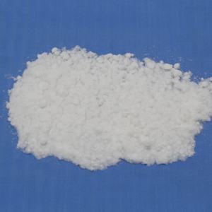
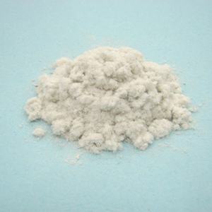
Spherical silica refers to silicon dioxide (SiO ₂) fragments engineered with an extremely consistent, near-perfect spherical form, identifying them from traditional uneven or angular silica powders stemmed from natural resources.
These particles can be amorphous or crystalline, though the amorphous type dominates industrial applications due to its remarkable chemical security, lower sintering temperature level, and absence of phase changes that could cause microcracking.
The round morphology is not naturally common; it has to be artificially attained through regulated processes that regulate nucleation, development, and surface energy minimization.
Unlike crushed quartz or merged silica, which show rugged sides and wide size circulations, round silica functions smooth surfaces, high packing density, and isotropic behavior under mechanical anxiety, making it perfect for accuracy applications.
The bit size typically ranges from 10s of nanometers to a number of micrometers, with tight control over size distribution enabling foreseeable efficiency in composite systems.
1.2 Managed Synthesis Paths
The main approach for producing round silica is the Stöber process, a sol-gel method developed in the 1960s that entails the hydrolysis and condensation of silicon alkoxides– most commonly tetraethyl orthosilicate (TEOS)– in an alcoholic solution with ammonia as a catalyst.
By adjusting criteria such as reactant concentration, water-to-alkoxide ratio, pH, temperature, and reaction time, researchers can precisely tune particle size, monodispersity, and surface area chemistry.
This technique yields highly consistent, non-agglomerated spheres with excellent batch-to-batch reproducibility, necessary for high-tech production.
Alternate approaches include flame spheroidization, where uneven silica fragments are melted and reshaped into balls by means of high-temperature plasma or fire treatment, and emulsion-based strategies that allow encapsulation or core-shell structuring.
For massive industrial production, salt silicate-based precipitation courses are additionally utilized, providing affordable scalability while preserving appropriate sphericity and pureness.
Surface area functionalization during or after synthesis– such as grafting with silanes– can present natural groups (e.g., amino, epoxy, or plastic) to enhance compatibility with polymer matrices or allow bioconjugation.
( Spherical Silica)
2. Functional Residences and Performance Advantages
2.1 Flowability, Loading Thickness, and Rheological Behavior
Among the most considerable advantages of spherical silica is its premium flowability contrasted to angular equivalents, a residential property critical in powder handling, injection molding, and additive production.
The absence of sharp edges decreases interparticle friction, allowing dense, uniform loading with marginal void area, which enhances the mechanical integrity and thermal conductivity of final compounds.
In electronic packaging, high packing density straight equates to decrease material content in encapsulants, enhancing thermal stability and decreasing coefficient of thermal expansion (CTE).
Additionally, spherical fragments convey positive rheological properties to suspensions and pastes, reducing viscosity and protecting against shear enlarging, which makes sure smooth dispensing and uniform covering in semiconductor fabrication.
This controlled circulation habits is crucial in applications such as flip-chip underfill, where precise material placement and void-free filling are required.
2.2 Mechanical and Thermal Security
Spherical silica displays exceptional mechanical toughness and flexible modulus, contributing to the support of polymer matrices without causing stress focus at sharp edges.
When included into epoxy resins or silicones, it improves hardness, put on resistance, and dimensional security under thermal biking.
Its reduced thermal development coefficient (~ 0.5 × 10 ⁻⁶/ K) closely matches that of silicon wafers and printed circuit boards, reducing thermal inequality tensions in microelectronic devices.
Additionally, round silica preserves structural integrity at raised temperatures (approximately ~ 1000 ° C in inert environments), making it ideal for high-reliability applications in aerospace and auto electronics.
The mix of thermal stability and electric insulation additionally improves its utility in power modules and LED packaging.
3. Applications in Electronic Devices and Semiconductor Sector
3.1 Duty in Electronic Packaging and Encapsulation
Round silica is a foundation material in the semiconductor sector, primarily utilized as a filler in epoxy molding compounds (EMCs) for chip encapsulation.
Changing conventional uneven fillers with round ones has actually revolutionized product packaging modern technology by making it possible for greater filler loading (> 80 wt%), enhanced mold flow, and lowered cord sweep throughout transfer molding.
This advancement sustains the miniaturization of integrated circuits and the growth of sophisticated packages such as system-in-package (SiP) and fan-out wafer-level packaging (FOWLP).
The smooth surface of round particles likewise lessens abrasion of fine gold or copper bonding wires, enhancing tool dependability and return.
In addition, their isotropic nature guarantees consistent tension circulation, minimizing the risk of delamination and cracking throughout thermal cycling.
3.2 Use in Sprucing Up and Planarization Procedures
In chemical mechanical planarization (CMP), spherical silica nanoparticles act as unpleasant agents in slurries created to brighten silicon wafers, optical lenses, and magnetic storage space media.
Their consistent shapes and size guarantee consistent product elimination rates and very little surface area issues such as scrapes or pits.
Surface-modified round silica can be tailored for specific pH atmospheres and sensitivity, boosting selectivity between different materials on a wafer surface.
This accuracy makes it possible for the manufacture of multilayered semiconductor frameworks with nanometer-scale flatness, a prerequisite for sophisticated lithography and tool integration.
4. Arising and Cross-Disciplinary Applications
4.1 Biomedical and Diagnostic Utilizes
Beyond electronics, round silica nanoparticles are increasingly utilized in biomedicine due to their biocompatibility, convenience of functionalization, and tunable porosity.
They serve as medication shipment service providers, where healing representatives are packed into mesoporous structures and launched in reaction to stimuli such as pH or enzymes.
In diagnostics, fluorescently identified silica spheres serve as stable, non-toxic probes for imaging and biosensing, surpassing quantum dots in particular biological atmospheres.
Their surface can be conjugated with antibodies, peptides, or DNA for targeted detection of pathogens or cancer biomarkers.
4.2 Additive Manufacturing and Compound Products
In 3D printing, particularly in binder jetting and stereolithography, round silica powders enhance powder bed thickness and layer uniformity, resulting in higher resolution and mechanical strength in printed porcelains.
As a reinforcing stage in metal matrix and polymer matrix composites, it improves rigidity, thermal administration, and put on resistance without compromising processability.
Study is also discovering hybrid particles– core-shell frameworks with silica coverings over magnetic or plasmonic cores– for multifunctional materials in picking up and energy storage.
In conclusion, spherical silica exemplifies how morphological control at the micro- and nanoscale can change a typical product into a high-performance enabler throughout diverse innovations.
From guarding microchips to progressing clinical diagnostics, its unique combination of physical, chemical, and rheological residential or commercial properties continues to drive development in science and engineering.
5. Provider
TRUNNANO is a supplier of tungsten disulfide with over 12 years of experience in nano-building energy conservation and nanotechnology development. It accepts payment via Credit Card, T/T, West Union and Paypal. Trunnano will ship the goods to customers overseas through FedEx, DHL, by air, or by sea. If you want to know more about silicon is a semiconductor, please feel free to contact us and send an inquiry(sales5@nanotrun.com).
Tags: Spherical Silica, silicon dioxide, Silica
All articles and pictures are from the Internet. If there are any copyright issues, please contact us in time to delete.
Inquiry us
